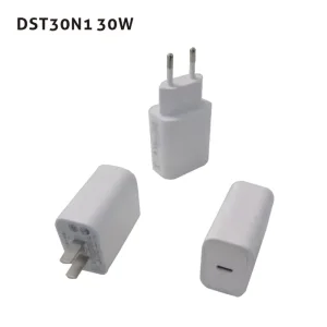
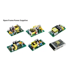
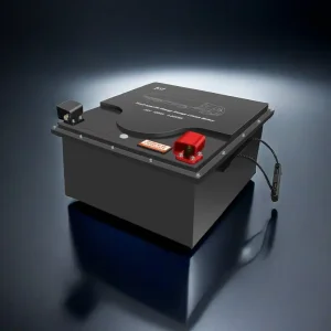
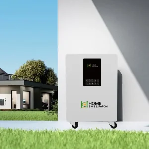
Discover our primary selection of enterprise-grade energy storage systems and specialized charging components, engineered for efficiency and long-term durability.
An industry-leading deep dive into B2B procurement strategies, GaN semiconductor evolution, and global compliance regulations governing laptop charging architectures.
GaN semiconductors replace traditional silicon, increasing switching speeds, boosting power density, and reducing physical unit sizes by up to 50% without thermal overload.
Intelligent power negotiation (PPS) ensures that multi-port laptop chargers dynamically allocate precise wattages, protecting delicate device batteries while maximizing charging speeds.
Top factories guarantee full international compliance, ensuring products carry UL, CE, FCC, RoHS, and CB certifications, allowing seamless market distribution.
A detailed technical comparison explaining the efficiency metrics and thermal management properties that define modern laptop charger factories.
| Performance Metric | Legacy Silicon Chargers | First-Generation GaN | Advanced GaN III / GaN Fast Pro |
|---|---|---|---|
| Power Conversion Efficiency | 85% - 88% | 90% - 92% | 94% - 96.5% |
| Switching Frequency | 50 kHz - 100 kHz | 200 kHz - 300 kHz | 500 kHz - 1 MHz+ |
| Thermal Dissipation Rate | Moderate (Requires massive heatsinks) | High (Reduced volume heatsinks) | Ultra-High (Automated power-down & premium gel coating) |
| Volume-to-Power Ratio | Low (Large form factor, heavy footprint) | Good (approx. 30% smaller than legacy) | Exceptional (Up to 55% space savings, ultra-slim designs) |
| Transient Load Response | Standard | Accelerated | Real-Time Auto-Negotiation (0.01s latency) |
Our dedication to environmental responsibility, strict manufacturing standards, and strategic global alliances ensures high-quality product delivery.

We operate with honesty and transparency in all our business dealings.

We are committed to pushing the boundaries of renewable energy technology to create a greener future.

We strive for everything we do from product development to customer service.

We believe that teamwork and partnership are most important for partners.
How our factories control failure rates and ensure global compliance across European, North American, and Asian markets.
We test all incoming capacitors, GaN controller chips, and PCB baseboards against tolerance profiles using computerized parameter analyzers before assembly begins.
Post-SMT reflow soldering, AOI scanners examine every solder joint for micro-fractures, voids, or misalignments, reducing human error rates to zero.
Every finished charger undergoes a full-load burn-in test inside specialized thermal chambers for 4 hours to catch any early component failures before shipping.
We run EMI testing on all adapter casings to guarantee compliance with FCC Class B and EN55032 standards, keeping line noise to a minimum.
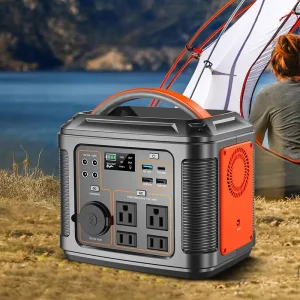
Connecting smart power adapters to larger energy grids, micro-storage networks, and portable power stations.
Frequently asked questions concerning factory lead times, engineering tooling, dynamic power profiles, and minimum order requirements.
For customized OEM/ODM housing designs, branded packaging, or specific localized AC plug configurations, the standard minimum order quantity (MOQ) is generally 1,000 units. For off-the-shelf standard designs, we can support smaller trial runs of 500 units to help partners validate their local markets.
Our chargers feature built-in smart controller chips that support the PPS (Programmable Power Supply) protocol. These chips communicate with connected laptops to adjust voltage and current dynamically in real-time. Additionally, they include hardware-level protection against over-voltage (OVP), over-current (OCP), over-temperature (OTP), and short-circuits (SCP).
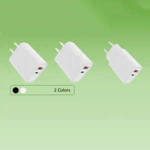
Yes. We supply interchangeable wall plug heads and regional pin configurations (US, EU, UK, AU, CN, KR, JP). We also offer custom packaging design, graphic layout alignment, and user manual translations to ensure your products are retail-ready.
High-wattage products undergo strict testing: initial component checking (IQC), automated optical inspection (AOI) after soldering, functional calibration, and a 100% full-load burn-in test at 40°C ambient temperature. We also perform regular drop tests, salt spray tests on metal parts, and EMI scanning to guarantee long-term reliability.
For standard designs with custom branding, our typical lead time is 25 to 30 days after proof approval. For completely new ODM projects requiring new enclosure tooling, the timeline ranges from 60 to 75 days, which includes prototype testing, verification cycles, and safety certification approvals.
Our 2022 strategic cooperation agreement with US partners has helped us refine our optical storage and charging systems to meet strict Western energy standards. This allows us to share research insights and supply chain benefits across all our product lines, including laptop chargers, energy storage, and industrial equipment.
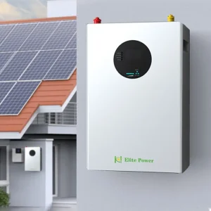
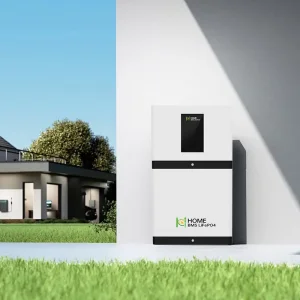
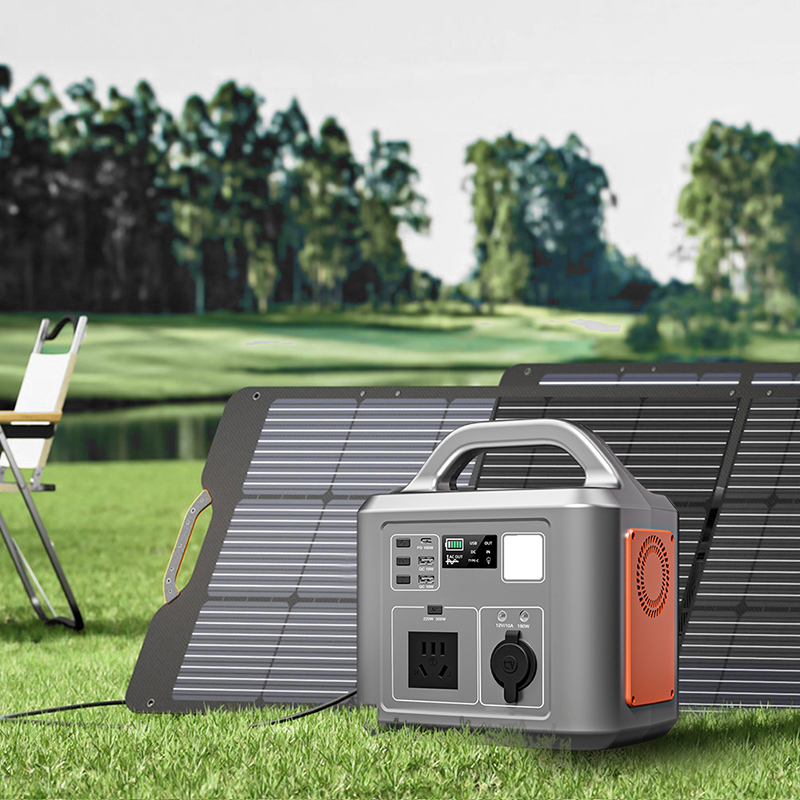
Explore our range of portable solar systems, localized residential storage, and smart charging technologies designed for demanding applications.